Construction of the SiPFAB pilot line for chip packaging at Tampere University to begin in May 2026

SiPFAB is part of the EU:n Chips Act programme, which aims to strengthen Europe’s competitiveness and resilience in the semiconductor industry. Tampere University has been granted €40 million in funding over five years through the programme to implement the pilot line.
“SiPFAB will place Tampere University at the heart of Finnish and European semiconductor expertise. This investment enables research and development activities on an entirely new scale and strengthens the vitality of the entire region,”
says President Keijo Hämäläinen.
Hämäläinen notes that Tampere has decades of experience in microelectronics research and chip design.
“We have expertise and a tradition of collaboration that does not emerge overnight. Tampere has built a strong ecosystem where education, research, and companies operate side by side. That is why it is excellent that we are now also developing new infrastructure that supports the advancement of the field.”
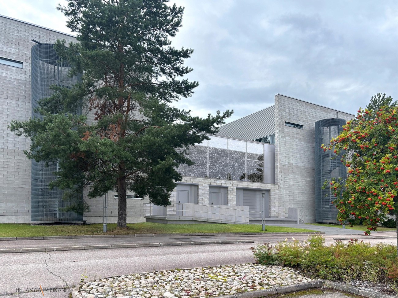
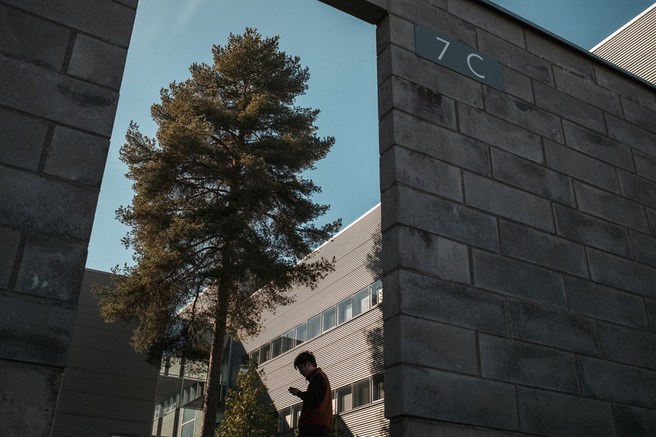
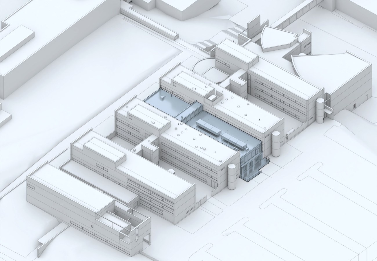
Cleanroom facilities to be built in the Festia building
The SiPFAB pilot line requires approximately 1,200 gross square meters of cleanroom space, along with related technical and staff facilities. In total, the project will cover approximately 2,800 gross square meters. Based on location studies, the pilot line was decided to be placed in the Festia building, combining extensive renovation with new construction.
The decision supports the long-term space utilization strategy of the Hervanta campus and also enables future expansion.
“The Festia solution provides us with the technically optimal and future-proof, scalable location on the university campus. It enables close, long-term collaboration with research groups and creates excellent conditions for strengthening industry collaboration and high-level fundamental research,” says SiPFAB Director Tuomas Lahtinen.
Construction to begin in 2026 – operational in 2027
Construction will begin in two phases on May 4 and July 1, 2026, as premises become available for the project. The construction and commissioning period is estimated at 11 months, with completion scheduled for April 1, 2027. Once completed, approximately 50 individual pieces of equipment for packaging, reliability testing, and characterization will be installed in the cleanroom. These will enable the development of new packaging solutions and chip technologies.