Photonics researchers are developing semiconductor chips for miniaturised optical systems

In December 2022, Nouman Zia received his PhD with a thesis concerning the development of chip-scale light sources. His doctoral dissertation focused on the integration of III-V semiconductor and silicon technologies for miniaturised light sources to be used in compact optical gas systems.
Now, he continues his research on deploying these chips for light-based gas sensors as a postdoctoral researcher in a study that brings together the Optoelectronics Research Centre (ORC) at Tampere University, the VTT Technical Research Centre of Finland, and Vaisala, a global leader in weather, environmental, and industrial measurement solutions.
According to Zia, integrated light sources operating at mid-infrared wavelength are needed because of the high demand for compact sensors in gas detection and medical diagnostics. However, the applications are not limited to sensing, and similar concepts can be deployed in other wavelength domains. Such an integrated light source platform can be harnessed to enable, for example, innovative light-based solutions in the field of quantum photonics or on-chip high-speed optical communication in data centres.
Combining semiconductor light sources and PICs
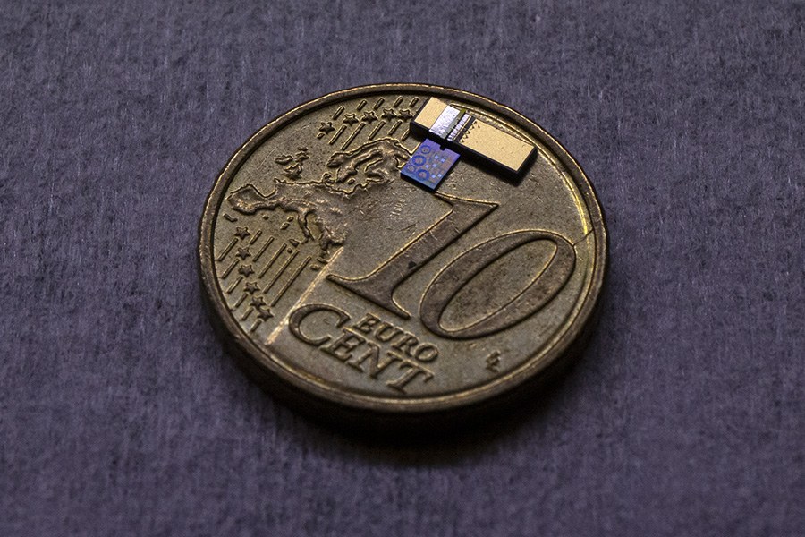
The existing gas-sensing solutions are either bulky or expensive or both. In the new research, the team is developing light-based sensors by bringing together compound semiconductor light sources – an area of internationally recognised expertise at Tampere University – and silicon photonics integrated circuits (PICs) which act as an integration platform that enables miniaturisation.
In general, semiconductor technology enables volume-scaling and an implicit cost reduction, power efficiency and system-on-chip integration. These features have given rise to a true industrial revolution in microelectronics. Expansion to the optical domain of integration technology would give way to new types of functionalities. For example, integrated light-based sensors at long wavelengths would make possible faster and more sensitive detection of gases due to the strong absorption of gas molecules in this wavelength region.
“The integrated light sources developed in our study are becoming the key component of a micro gas sensor. The proof-of-concept gas sensor will be demonstrated with partners in the next phase of this project,” Zia says.
An efficient consortium with clear responsibilities
In the research consortium, each player has unique expertise.
“Tampere University’s research team is developing state-of-the-art III-V light-emitting devices and an advanced testing facility for chips is created in the study. VTT is at the leading edge of silicon manufacturing and its thick silicon PIC platform enables practical integration with ORC’s III-V technology. For its part Vaisala will provide the inputs for practical validation of the silicon-based miniaturised gas sensor,” Zia explains.
The ORC research group implements a full R&D value chain of semiconductor optoelectronics components. This starts from the design of application-specific semiconductor structures, followed by the fabrication of semiconductor wafers (in this case GaSb-based), the clean-room processing of components, sub-system development, and finally a proof-of-concept application.
The group is headed by Professor Mircea Guina, who was also the responsible supervisor of Zia’s thesis. Adjunct Professor Jukka Viheriälä coordinates the semiconductor device fabrication. Zia’s role is to design, fabricate and test semiconductor chips. He is also responsible for their integration with silicon PICs. Other team members, Heidi Tuorila and Samu-Pekka Ojanen are involved in developing PICs, proof-of-concept gas sensors, and the processing of the semiconductor chips.
The initial developments were started in a collaboration between the partners under the MIREGAS project funded by Horizon 2020 and the RAPSI and PICAP co-innovation projects funded by Business Finland. The work is also linked to the Academy of Finland-funded PREIN Photonics Flagship project.
First place in Huawei silicon photonics contest for PhD students
In December 2022, Huawei awarded Zia for his research achievements.
The Huawei Silicon Photonics PhD Student Contest 2022 was targeted at PhD students and Postdocs studying at European universities. The contest covered topics related to silicon photonics technologies in areas such as hybrid integration, electronic-photonic codesigns, lidar, sensing, and co-packaged optics. Among the 10 finalists, Zia presented his research at a Huawei R&D centre in Belgium.
The jury was convinced, for example, by the quality and thoroughness of Zia’s research as well as the innovation and commercial potential of his solutions.
“It is a wonderful feeling to get international recognition for my research work. I feel that I am working on something that is adding value to human life,” Zia says.
Further information
Nouman Zia
+358 40 826 2484
nouman.zia [at] tuni.fi


