Tampere University is at the forefront of semiconductor chips research and education – close industry collaboration plays a key role

Tampere University has a long-standing tradition of researchers collaborating with companies to develop new technologies. Strong industry collaboration is also a hallmark of the University’s semiconductor chips research and education – areas in which Tampere is both a forerunner and a leading hub of expertise in Finland.
“We are building a common direction through continuous dialogue, sharing views on what is meaningful and what is worth investing in,” says Professor of Electronics Matti Mäntysalo.
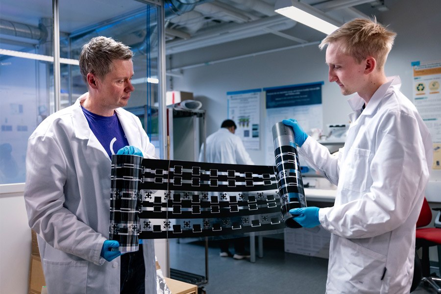
A substantial number of chip design and development projects are conducted in cooperation with, or funded by, industry partners at Tampere University.
Innovations are created, protected and transferred to industry, and several successful chip start-ups have emerged from the University.
First-hand insight into industry needs also enables the University to prioritise relevant content in its teaching.
SoC Hub brings together system-on-chip developers
The System-on-Chip (SoC) Hub is a prime example of what can be achieved through university-industry collaboration.
Established in 2020, the SoC Hub brings together research groups, students and companies focused on the development of system-on-chips.
“Without strong industry involvement and a shared vision, we would have had limited resources to establish the SoC Hub on our own. This initiative has had a remarkable start and has already attracted tens of millions of euros in research funding,” says Timo Hämäläinen, Professor of Computer Engineering and Head of the SoC Hub.
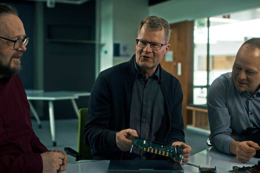
The electronics and computer industries emerged in Tampere early on, with the University developing these technologies in close collaboration with industry.
Hämäläinen believes that the combination of expertise across disciplinary boundaries will provide an important competitive advantage for Tampere University in the future.
“While opportunities for collaboration have always existed, multidisciplinary collaboration is now explicitly recognised as a priority for the University.”
Laser-based data transmission powers the future of AI
Chips are commonly thought of as small silicon-based electronic devices used for processing and storing data.
However, in our daily lives we also rely on optoelectronic chips that generate or detect light. These include laser chips that are used, for example, in smartphone facial recognition, telecommunication optical fibre links and in high-speed data transmission in data centres.
“Laser light travels without generating heat and enables extremely efficient transmission of large volumes of data. Nowadays we see a major push to use such optical interconnects to reduce the energy-consumption in data centres and enable future AI infrastructure, for example,” says Mircea Guina, Professor of Optoelectronics at Tampere University.
The production of optoelectronic chips requires specialised semiconductor materials that do not occur naturally and must be engineered. According to Guina, Tampere University offers an exceptional research infrastructure for studying and manufacturing these materials.
Guina also commends the University’s unique culture of encouraging researchers to develop practical applications. Research conducted at the Optoelectronics Research Centre (ORC) research group has already led to the creation of nine start-ups with strong focus on advanced laser technologies and leading positions in a wide range of applications.
“Our vision starts from fundamental research enabling strong differentiation, but then we distinguish by pursuing also applied research and foster technological innovation,” concludes Guina.
SiPFAB supports the commercialisation of new technology
The System-in-Package Fabrication (SiPFAB) pilot line, currently under construction at Tampere University, exemplifies the integration of different areas of expertise. System-in-package fabrication is a process in which delicate semiconductor chips are enclosed within protective packages incorporating all the required electrical connections.
Approximately 1,300 square metres of new cleanroom space is being constructed on the Hervanta campus for piloting, packaging and testing novel semiconductor technologies. The University has received €40 million in funding for the SiPFAB project, with half provided under the EU’s Chips Act and half by Business Finland.

The construction of the cleanroom facilities commenced recently and is scheduled for completion in the spring of 2027, followed by equipment installation. The facilities are expected to be up and running in late 2028.
According to SiPFAB Director, Dr Tuomas Lahtinen, recruitment is also underway: the SiPFAB team currently employs five staff members, with plans to expand to approximately 20.
More information
Author: Virpi Ekholm


