Tuomas Lahtinen leads the SiPFAB pilot line in advancing next-generation chip technologies

Tuomas Lahtinen, PhD (Applied Physics), was appointed Director of the System-in-Package Fabrication (SiPFAB) pilot line at Tampere University in April 2025. The cleanroom facilities required for the pilot line are currently under construction in the Festia building on the Hervanta campus. SiPFAB is part of a Europe-wide semiconductor infrastructure spanning seven countries, aimed at strengthening semiconductor expertise across the continent.
The pilot lines provide companies with access to advanced facilities for process development and testing. Other pilot lines in the network focus on chip manufacturing and the development of new semiconductor materials, while the SiPFAB pilot line in Tampere specialises in chip packaging. But what do the terms SiPFAB and chip packaging actually mean?
“SiPFAB stands for system-in-package fabrication, which involves physically enclosing semiconductor chips with a range of built-in functionalities into a single protective package. This package provides access to their functions while shielding them from external conditions. In essence, the entire system is combined into one compact unit,” says Lahtinen.
In everyday language, the term “chip” generally refers to semiconductor devices used for computing purposes. The growing demand for semiconductor chips is driven by technologies such as artificial intelligence (AI), which rely on them. The world’s most advanced high-performance semiconductor chips are currently manufactured by the Taiwan-based company TSMC.
“Packaging is becoming increasingly important because the most powerful chips are also extremely valuable. Packaging is one way to address this challenge. Previously, multiple functions were integrated onto a single chip, but the current trend is to combine several specialised chips within a single package. This means that cutting-edge components can be produced in Taiwan, while other functional elements can be manufactured elsewhere.”
The global shift towards electrification is also increasing the demand for semiconductor chips. There is also a growing need for power semiconductors, which are used not for computation but for converting electrical energy.
“For example, in an electric vehicle, the battery operates on direct current (DC), while the motor requires alternating current (AC). The conversion from DC to AC is carried out using semiconductor chips. Similar technologies are used in renewable energy systems, where electricity generated by wind farms must be converted into a form compatible with the power grid. This is one of the key application areas for the SiPFAB pilot line.”
In practical terms, chip packaging involves creating electrical connections that are as energy-efficient as possible and capable of withstanding heat or environmental conditions, depending on the intended use of the chips.
“The power consumption of AI chips is currently around one kilowatt and continues to rise. Supplying such a massive amount of power to a chip is far from straightforward. Once the computations have been completed, the resulting data must be extracted from the chip. This is traditionally achieved using electrical signals, but in the future, alternative methods such as light-based transmission may offer greater energy efficiency. The reliability of these connections is also critical. For example, when offshore wind farms are constructed far from shore, the aim is to ensure their uninterrupted operation for decades with minimal maintenance.”
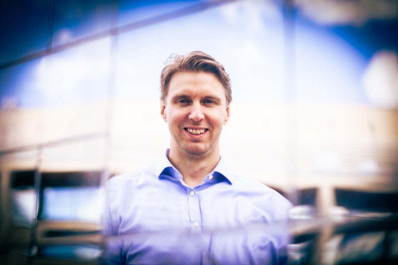 Photo: Jonne Renvall
Childhood spent in Qatar, master’s degree completed in London
Tuomas Lahtinen became interested in semiconductor chips while working on his PhD thesis, which explored magnetic and ferroelectric materials and was completed in 2013.
“I carried out my doctoral research at Aalto University, which has extensive cleanroom facilities. That is where I produced my samples and first became involved in the semiconductor field.”
Before this, Lahtinen had attended school and studied in several countries around the world. His parents worked in computer maintenance, and in 1990, when Lahtinen was still very young, the family relocated to Kuwait for work.
“At the time, maintaining computers was still standard practice. We only spent three months in Kuwait before Iraq invaded the country, and we had to flee back to Finland.”
As Finland was in the grip of recession, his parents soon returned to the Middle East, this time settling in Qatar. The family lived there for 13 years, and Lahtinen completed his comprehensive and upper secondary education within the British school system. After finishing school, he returned to Finland to complete his national service and subsequently continued his studies at Imperial College London.
“I originally set out to study theoretical physics but found it too theoretical for me. I have always enjoyed working with my hands. Between software and hardware, I definitely prefer hardware. I switched to experimental physics, and that has proved to be the right choice.”
Lahtinen points out that career paths may not always be immediately clear to physics graduates but tend to become clearer once they identify their specific field of interest.
After years of living abroad, Tampere has felt just the right size as a city.
“Tampere is very pleasant and large enough to have plenty going on. I have really enjoyed living here.”
Process development turns abstract ideas into practical solutions
After finishing his PhD, Lahtinen embarked on a career in industry. He has worked at three companies, developing expertise across all stages of the chip packaging process.
This industry background is valuable in his current role as Director of SiPFAB, as the pilot line will involve extensive collaboration with companies. The first five years of operation will be funded by Business Finland and the EU’s Chips Joint Undertaking (Chips JU), after which the aim is to secure industry funding to cover at least part of the budget.
“Companies will use SiPFAB, and they need to be able to rely on long-term collaboration with us. The pilot line is here to stay.”
Lahtinen currently leads a small team of five, but the aim is to expand it to 20.
“Even that is not a large number, given the scale of the pilot line. In addition, there will be users from industry and academia.”
Alongside the construction of the facilities and the recruitment of new team members, SiPFAB is currently assessing industry needs and inviting competitive tenders for research equipment. Once the equipment has been installed, it can be tested, and the development of the pilot line’s own process flows can begin. Reaching the process development phase may take until the end of 2028, but this is the stage Lahtinen is most looking forward to.
“That is when the work and ideas really begin to take shape. It is the most interesting phase and always an opportunity to learn.”

SiPFAB
System-in-Package Fabrication (SiPFAB) is being established on the Hervanta campus to bring chip packaging, integration, and testing together under one roof. The facility will combine Wide Band Gap (WBG) chips and other semiconductor components into complete system solutions. The pilot line will provide researchers and industry partners with a unique environment for exploring sustainable, future-oriented technologies and advancing ideas from concept to prototype.
As part of the ChipsJU WBG Pilot Line, SiPFAB will also contribute to strengthening the European semiconductor ecosystem. The infrastructure is currently under development and will become operational in stages between 2027 and 2028 as equipment installation progresses.
Author: Eli Harju


