Embedding Brains in Materials: Dr. Amit Tewari on the Next Frontier of Flexible Neuromorphic Electronics

Today's computing is bottlenecked by a historical divide where memory is stored in one physical location and computation is executed in another. While silicon chips are incredibly powerful and efficient, standard wearable devices must constantly transmit raw data back and forth to central servers to process information, a transmission process that consumes high amounts of power. In our era of wearable health monitors, soft robotics, and smart environments, solving this bottleneck requires brain-inspired processing. However, bringing these advanced architectures to the human body demands a shift from physically rigid silicon platforms to flexible, conformable materials.
Dr. Amit Tewari, recently appointed as a Senior Research Fellow at the Tampere Institute for Advanced Study, aims to collapse this divide. His three-year fellowship establishes an independent research program targeting the physical bottlenecks of modern hardware, starting with a fundamental manufacturing limitation.
"My project, 2D-NEURO, addresses a fundamental challenge, that is how to bring brain-inspired computing from conventional rigid silicon platforms to flexible and wearable systems. While neuromorphic devices have shown great promise, manufacturing them on soft substrates remains difficult because the high temperatures normally required for device fabrication can damage flexible materials."
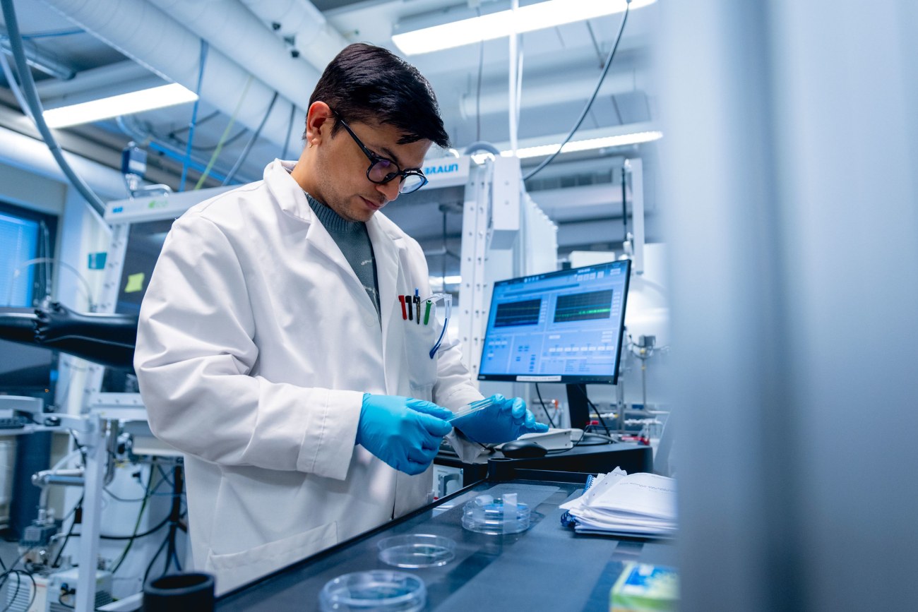 Photo: Karu Films
The Physics of Synaptic Materials
In biological brains, learning occurs when the physical connections between individual neurons, called synapses, strengthen or weaken based on use. Replicating this dynamic behavior in physical hardware requires specialized electronic components.
While a standard resistor simply controls electrical flow, a memristor remembers the history of current passing through it. Combined with a transistor, it forms a hybrid component called a memtransistor. These devices act as artificial synapses, performing memory storage and signal processing within a single component.
Achieving this brain-like architecture on soft surfaces requires moving away from the thick, rigid silicon used in standard computer chips, opting instead for two-dimensional (2D) semiconductors.
"Because these materials are only a few atoms thick, they offer unique advantages including mechanical flexibility, excellent electrical control, high sensitivity, and tunable electronic properties."
These characteristics make them particularly well suited for building electrical components capable of mimicking biological learning.
"Like biological synapses, memtransistors can adjust and retain their conductance based on previous signals, enabling learning and memory functions directly within the device."
Integrating these atomic-scale semiconductors with low-temperature insulating films (dielectrics) bypasses the constraints of silicon fabrication. This results in a lightweight, flexible platform capable of simultaneous sensing, memory storage, and real-time computation.
Manufacturing with Light: High-Photonic-Sintering
While promising, translating 2D materials onto flexible substrates like plastics, paper, or elastomers presents a major hurdle. Standard semiconductor manufacturing relies on high-temperature furnace baking to eliminate defects, which easily exceeds several hundred degrees Celsius and melts flexible substrates. To resolve this, the project utilizes high-photonic-sintering (HPS), an innovative technique replacing slow furnaces with localized light energy.
"The physics is simple: the deposited dielectric film absorbs the light and heats up for only a fraction of a second, enabling atomic rearrangement, defect reduction, and improved material quality. Because the heating is highly localized and extremely brief, the flexible substrate remains relatively cool and avoids thermal damage."
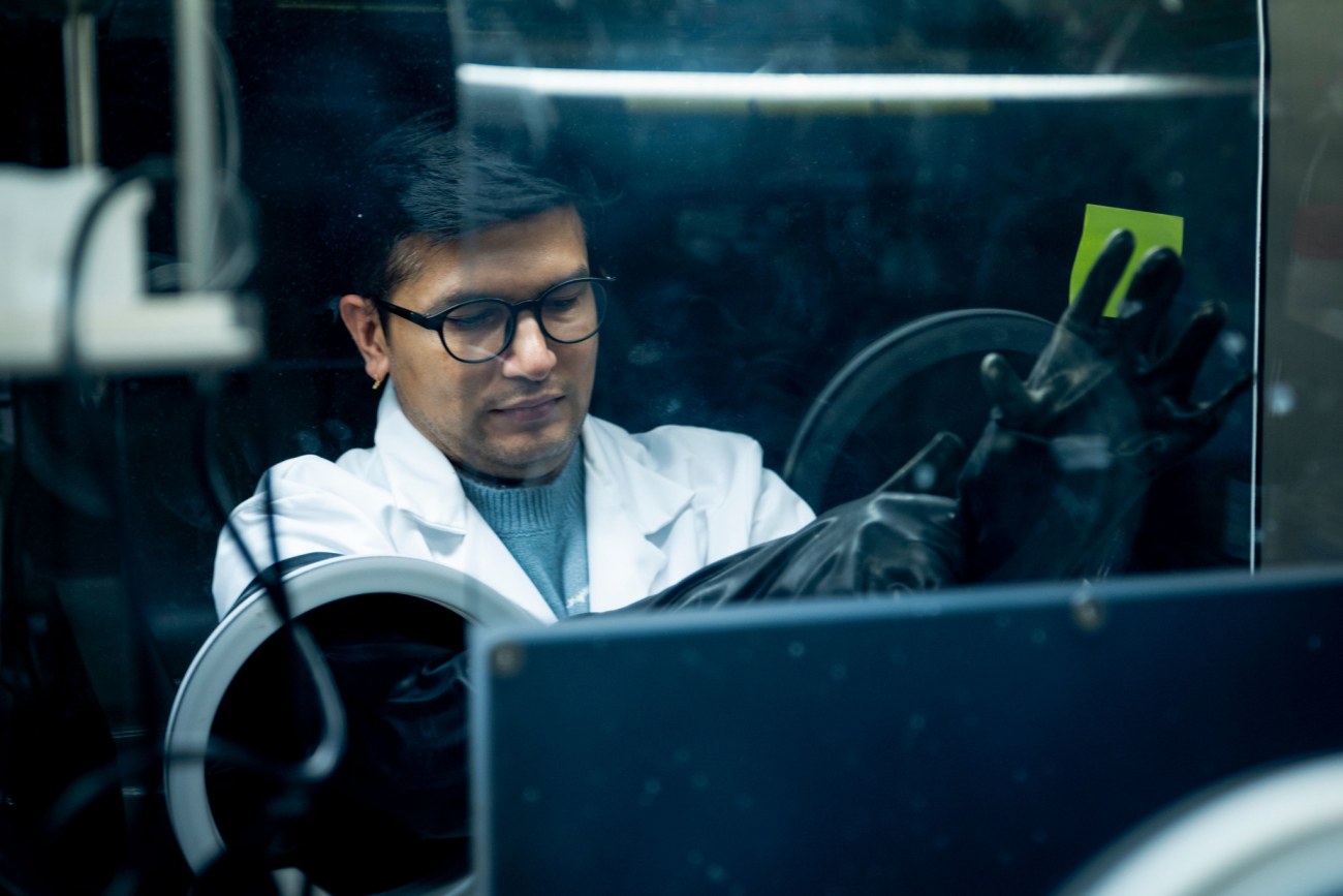 Photo: Karu Films
Localized Intelligence at the Point of Contact
Overcoming the dependency on rigid silicon allows for conformable electronics that adhere seamlessly to irregular, soft surfaces like human skin or textiles. Today's wearables function as simple pipelines, gathering raw data and broadcasting it to remote servers; creating major processing delays and power demands. Processing information locally at the point of contact mimics a biological nervous system.
"Instead of transmitting large amounts of raw data to external processors, these circuits can process information locally, much like biological nerves and synapses. The key advantage is lower power consumption, faster response times, and reduced data-processing bottlenecks, enabling real-time decision-making for applications such as healthcare monitoring, human-machine interfaces, and soft robotics."
A Convergence of Disciplines
Dr. Tewari's academic journey reflects this rich blend of chemistry, device physics, and materials engineering. His doctoral research, conducted jointly at IIT Bombay and Monash University, focused on developing graphene-based inks and flexible health sensors, establishing his foundation in nanomaterials. He then transitioned to device physics during a research appointment at KAIST in South Korea, where he investigated energy-efficient ferroelectric memory. This specialized technology stores data using electrical polarization within thin films of hafnium zirconium oxide (HfZrO2). Later, as a researcher at Åbo Akademi University in Finland, he bridged these fields with bioelectronics, exploring how synthetic electronic components can interface directly with living biological signals.
"In my daily work, I move between material synthesis, device fabrication, characterization, and circuit level thinking. This continuous exchange between disciplines is one of the most exciting aspects of modern engineering and is essential for developing next-generation neuromorphic technologies."
Now based at Tampere University, his research unites these technical threads within a collaborative regional ecosystem. Establishing this program relies heavily on local partnerships and shared infrastructure across the university, prompting a strong emphasis on mentorship.
"I would like to express my sincere gratitude to Prof. Matti Mäntysalo and Prof. Sayani Majumdar at Tampere University, as well as Prof. Paul Berger at The Ohio State University, for their invaluable guidance, unwavering support, and continued confidence in my work," notes Tewari, highlighting their collaboration on key initiatives, including the SOIL, Intellisence Cust., and HI-PHOTO-SINTER projects.
The Future of Printed Intelligence
Looking beyond the immediate three-year timeline of the 2D-NEURO project, the ultimate goal is to redefine processing power as an inherent, printable property of physical matter, rather than an external, centralized commodity. The vision is a future where brain-like processing circuits can be deposited onto everyday surfaces as easily as barcode labels are printed today.
"We envision surfaces that can not only sense their environment but also process information and respond in real time. Rather than simply collecting data, these surfaces could learn from their surroundings, recognize patterns, and make local decisions with very low power consumption."
 Photo: Karu Films
Electronics research centre (ERC)
Laboratory for Future Electronics (LFE)
Research fields
2D materials, Transistors (MOSFETs, OFET, EGOFETs, OECT), sensors (Physiological, Chemical and Bioelectronics), High-k dielectric materials, Ferroelectric Materials, and memory devices (MIM, MIS, MFM, MISM).
Author: Sujatro Majumdar


