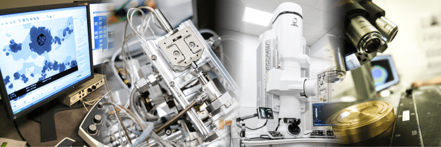
The Microscopy Center staff mainly trains people to use the instruments independently and provides support and training. We can also help you analyse your sample especially in cases where you need the more advanced techniques (TEM, FIB).
Please find the detailed policies depending on your affiliation
Policy and fees for external partners
Please contact the Microscopy Center staff at tmc [at] tuni.fi to learn more about analysing your samples with us.
Policy for users from Tampere University
The Microscopy Center staff mainly trains people to use the instruments independently and provides support and training. We can also help you analyse your sample especially in cases where you need the more advanced techniques (TEM, FIB).
Publishing results obtained at the Microscopy Center
When publishing results obtained at the Microscopy Center, please mention this in the acknowledgements, prefereably using the following phrase:
“This work made use of Tampere Microscopy Center facilities at Tampere University.”
In addition, we request that you add Tampere Microscopy Center as Facilities/Equipment for that publication in TUNICRIS.
This allows us to monitor our contribution to the research community and helps us to gather funding to acquire new equipment.
Becoming a user
Potential new users should contact the Microscopy Center staff responsible for the instrument they are interested in to get detailed information on the training requirements and procedure. If you are interested in getting access to an SEM but don’t know which one, please contact tmc [at] tuni.fi. To speed up the process and help us tailor the training to match your needs, new users are encouraged to provide the following information when contacting the staff:
- Your research group and supervisor
- Instrument you are interested in
- Type of samples you plan to analyse (materials, sample size, etc)
- What type of information you are expecting to learn from your samples
- Estimated need for the measurements (frequency of measurements, duration of the measurement need if known)
Before gaining access to Microscopy Center you must complete the chemical safety course in Moodle and will receive additional safety training from the microscopy center staff.
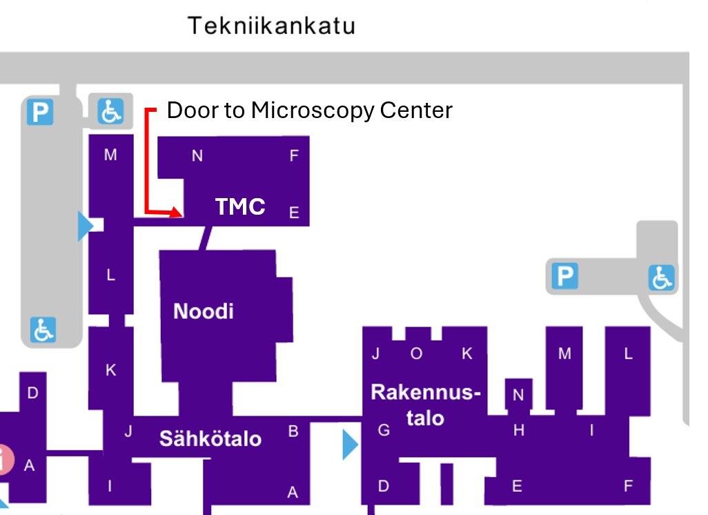
Booking of instruments is handled via https://tuni.agendoscience.com/
Electron microscopy
New users for any electron microscope should first pass the course MSE.410 Electron Microscopy or provide study records and course descriptions for previously completed studies of similar level performed elsewhere.
Users with substantial hands-on experience with electron microscopes can fulfil the requirements with description of said experience and demonstration during the training session. The SEM you will be trained on will depend on your needs and possible previous experience.
Typically, analysis techniques such as EDS or EBSD require an additional training session after the new user has become accustomed to the basic imaging with the SEM.
Fees
For researchers at Tampere University the use of the instruments is free. Advanced analysis that requires an operator from the Microscopy Center staff is free for testing of new ideas but for systematic analysis, a project number for work time allocation is required. We encourage research group leaders to contact us already when planning a new project that will make use of the instruments and staff in the Microscopy Center.